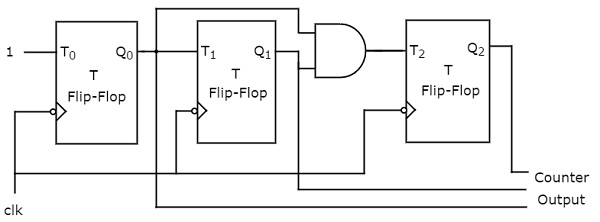
Block Diagram Of 4 Bit Synchronous Counter

Synchronous Counter And The 4 Bit Synchronous Counter

A 4 Bit Synchronous Counter Using T Flip Flops Download
Synchronous Counter Definition Working Truth Table Design
Asynchronous Counter Definition Working Truth Table Design

4 Bit Down Counter
Asynchronous Counter

Because this 4 bit synchronous counter counts sequentially on every clock pulse the resulting outputs count upwards from 0 0000 to 15 1111.
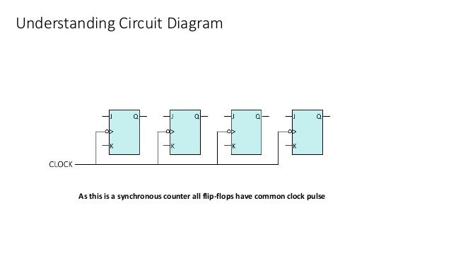
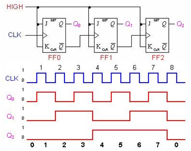
Block diagram of 4 bit synchronous counter. The flip flops are clocked at the same time by a common clock pulse. The below image is showing the timing diagram and the 4 outputs status on the clock signal the reset pulse is also shown in the diagram. This page of verilog source code section covers 4 bit binary synchronous reset counter verilog code the block diagram and truth table of 4 bit binary synchronous reset counter verilog code is also mentioned. 2 bit synchronous up counter.
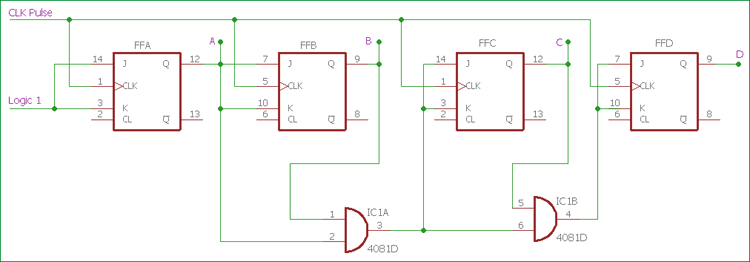
The circuit diagram of 4 bit synchronous counter by. Synchronous parallel counters synchronous parallel counters. We can modify the counting cycle for the asynchronous counter using the method which is used in truncating counter output. All these flip flops are negative edge triggered and the outputs of flip flops change affect synchronously.
Synchronous counter timing diagram in the above image clock input across flip flops and the output timing diagram is shown. The following diagram shows a sequential circuit that consists of a combinational logic block and a memory block. It is capable of counting numbers from 0 to 15. The basic block diagram of 4 bit sy nchronous.
The counting output across four output pin is incremental from 0 to 15 in binary 0000 to 1111 for 4 bit synchronous up counter. 2 bit synchronous binary counter using t flip flops or jk flip flops with identical j k inputs. The steps to design a synchronous counter using jk flip flops are. Asynchronous 4 bit up counter.
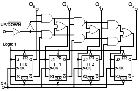
The j a and k a inputs of ff a are tied to logic 1. 4 bit binary synchronous reset counter verilog code. Design and analysis of 4 bit binary synchronous counter by leakage reduction techniques. The clock inputs of all flip flops are cascaded and the d input data input of each flip flop is connected to a state output of the flip flop.
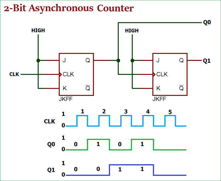
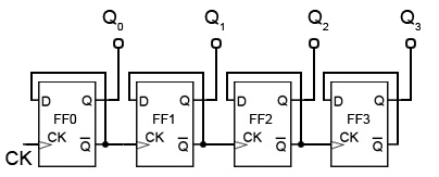
A 4 bit asynchronous up counter with d flip flop is shown in above diagram. We can design these counters using the sequential logic design process covered in lecture 12. If the clock pulses are applied to all the flip flops in a counter simultaneously then such a counter is called as synchronous counter. On each clock pulse synchronous counter counts sequentially.
The t inputs of first second and third flip flops. Therefore this type of counter is also known as a 4 bit synchronous up counter. However we can easily construct a 4 bit synchronous down counter by connecting the and gates to the q output of the flip flops as shown to produce a waveform timing. Creating the asynchronous counter example and usability.
So ff a will work as a toggle flip flop. The j b and k b inputs are connected to q a. You will learn to derive the combination logic that meets the design specifications.

3 Bit 4 Bit Up Down Synchronous Counter Youtube
4 Bit Binary Counter

Bidirectional Counter Up Down Binary Counter
Digital Counters
Synchronous Counter Design Online Digital Electronics Course
Ring Counters Johnson Ring Counter

Bcd Counter Using D Flip Flops

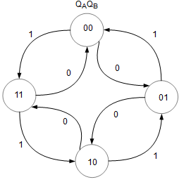
Design A 4 Bit Truncated Sequence Counter Using Jk Flip Flops

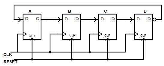
4 Bit Counter Using The Clear Input Download Scientific Diagram
Asynchronous Counter Sequential Logic Circuits Electronics
Digital Circuits Counters Tutorialspoint

Altera Cpld Basic Tutorial Case Synchronous Up Counter 4 Bit
Ripple Counter Circuit Diagram Timing Diagram And Applications
